When silicone chip packaging adhesives prevent solder joint cracking
by
Published
Views:
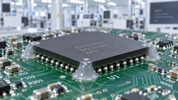
Solder joints crack when the package, board, and mounted component expand or move by different amounts while the joint is already carrying mechanical strain. Silicone chip packaging adhesives reduce that strain when they are placed where movement needs to be absorbed rather than transferred directly into balls, leads, or interconnect pads. Their value comes from low modulus, durable elasticity across a broad temperature range, and the ability to remain compliant after cure. Used in the right geometry, a silicone material can turn a concentrated stress point into a wider, lower-stress load path.
This is particularly relevant around BGAs, chip-scale packages, stacked assemblies, fine-pitch interconnects, and packages mounted on substrates with a very different coefficient of thermal expansion (CTE). A rigid package on an organic board may bend differently during thermal cycling. A large package has a greater distance from its neutral point, so its outer solder joints often see the highest shear displacement. Silicone does not eliminate the dimensional mismatch, but it can limit board flexure, package rocking, corner lift, and vibration-driven movement that accelerate fatigue.
Where compliant silicone changes the failure path
The same material can protect solder joints in several package-level configurations, but the intended mechanism must be clear before selection. A perimeter bead, corner bond, local strain-relief fillet, or conformal encapsulation does not impose the same mechanical boundary conditions. Applying a soft adhesive around a device is not automatically beneficial; excessive coverage, poor adhesion, voids, or an unsuitable cure profile can introduce new failure modes.
Corner bonding is often used to restrain package lift and reduce cyclic bending at BGA corners. Small deposits at selected corners can support the package without fully locking the entire underside. This approach is useful when the solder balls need added protection from shock, board flexing, or vibration but access for rework remains important. Deposit placement matters. A bead that extends too close to solder interconnects can contaminate pads, interfere with inspection, or create an unwanted stress concentration after cure.
Edge bonding distributes restraint along part of the package perimeter. It is appropriate when the device needs more continuous support than isolated corner dots can provide. The cured adhesive must remain sufficiently elastic at the lowest service temperature, because a material that stiffens sharply in cold conditions can transfer high stress back into the package edge and board surface.
Encapsulation or dam-and-fill protection is selected when moisture exclusion, vibration damping, electrical insulation, or protection of wire-bonded features is also required. Here, the material volume becomes more significant. A thick silicone layer can cushion the assembly, yet a deep cure, trapped volatiles, and heat released during cure require closer process control. Full encapsulation also changes serviceability much more than a corner-bond process.
Stress relief depends on more than a low-modulus data-sheet value
A low elastic modulus is a useful starting point, but it is not a complete predictor of solder-joint reliability. Modulus varies with temperature, strain rate, cure state, and test method. A value measured on a bulk specimen at room temperature does not describe the local response of a thin adhesive fillet exposed to rapid thermal transitions and repeated board bending. The relevant question is whether the cured adhesive stays compliant throughout the actual temperature and loading profile while retaining adhesion to the surfaces it contacts.
Elongation at break is also easy to overread. Very high elongation can indicate a flexible polymer network, but it does not prove that the adhesive will damp cyclic strain effectively or remain bonded after humidity and heat exposure. Tear resistance, stress relaxation, cohesive strength, and adhesion retention all influence the result. A soft material with weak cohesive integrity can crack within the bead. A highly extensible material that gradually detaches from the package wall may leave the solder joints exposed to the original movement.
CTE deserves the same context. Silicone materials often have a higher CTE than ceramic, silicon, metal leadframes, and many package substrates. That difference is not necessarily disqualifying because the silicone’s compliance allows it to deform. Problems arise when a heavily filled or unusually stiff formulation has enough modulus to turn its own thermal expansion into a significant force. Filler loading may improve thermal conductivity or reduce flow, but it can also raise viscosity, alter wetting, and reduce the stress-relief behavior that justified choosing silicone in the first place.
The interface often decides whether the adhesive protects anything
Silicone adheres differently to solder mask, organic solderability preservative areas, nickel-gold finishes, mold compound, ceramic, anodized metal, and polymeric package surfaces. Surface energy alone does not settle the issue. Mold-release residues, fingerprints, flux residues, cleaning-agent carryover, and absorbed moisture can all produce a bond that appears acceptable after initial cure but loses integrity during aging.
Package surfaces should be evaluated in the same condition in which they enter production. Testing a freshly cleaned coupon while the assembly line receives components stored in trays, handled repeatedly, and exposed to flux vapors gives an optimistic result. If plasma treatment, primer, or a controlled cleaning step is needed, its timing window needs to be part of the process definition. A treatment that improves adhesion immediately after activation may have little value after prolonged staging in an uncontrolled environment.
Silicone chemistry must also be compatible with nearby electronics. Some cure systems release small molecules during reaction, and some low-molecular-weight constituents can migrate under heat. Sensitive contacts, optical surfaces, switches, and unsealed cavities require specific compatibility evaluation rather than an assumption based on general silicone use. Electrical insulation properties should be considered after environmental exposure, not only on an unaged cured sample. Where corrosion-sensitive metals are present, the selected chemistry and any cure by-products need particular scrutiny.
Bead shape is a mechanical design variable
Dispense volume is frequently treated as a production setting, yet its final shape determines how the adhesive carries load. A narrow, tall bead may concentrate peel stress at its edges. A broad, shallow fillet can distribute load more smoothly but may spread into restricted areas. The target is a repeatable cured geometry with enough cross-section to support the package and enough compliance to deform without detaching.
Needle diameter, dispense pressure, valve opening time, material temperature, and thixotropy influence that geometry. A formulation that flows well on a flat coupon may wick under a package or slump across a solder-mask boundary on a warm production board. Conversely, a highly thixotropic paste can retain a precise dot but leave poor contact on rough mold compound unless the deposit is allowed to settle or is pressed into place within an appropriate assembly window.
Jet dispensing is useful where access is limited or very small deposits are needed, but high-speed placement does not remove the need to inspect wet-out. Satellite drops, inconsistent deposit height, nozzle contamination, and material stringing can create variability that is too small to notice visually yet large enough to alter package support. Weight verification, vision-based bead measurement, and periodic destructive cross-sections reveal different aspects of the process. No single inspection method establishes both correct volume and correct interface contact.
Cure conditions can either preserve or create stress
Silicone systems may cure through heat, moisture, addition reaction, or two-part mixing. The choice affects line design as well as reliability. A long room-temperature cure can preserve sensitive assemblies and avoid high thermal exposure, but it may require extended fixturing and can leave the package vulnerable to movement before sufficient green strength develops. Heat acceleration reduces cure time, although rapid heating can alter viscosity before gelation, move the deposit, or create thermal gradients across a mixed-material assembly.
For two-part formulations, mix ratio accuracy is not merely a handling issue. A ratio drift can change cure speed, hardness, adhesion, and the level of residual reactive species. Static mixer condition, cartridge age, material temperature, and purge volume need to be controlled so that early and late shots from a production run do not behave differently. With addition-cure silicones, catalyst inhibition from certain contaminants can leave localized uncured regions even when a bulk sample seems fully cured.
Residual stress should be assessed after the complete cure profile, including cooldown. A package constrained while the adhesive gels may retain a different stress state from one that is free to settle before cure. Board supports, clamps, fixture flatness, and placement force are therefore part of the adhesive application. An apparently flat board can be forced into curvature by an unsuitable fixture and released only after the adhesive has locked that distortion into the assembly.
Separate solder fatigue from look-alike failures
A crack observed near a solder joint does not always originate in solder fatigue. Interfacial pad separation, laminate cracking, via damage, package warpage, brittle underfill fracture, or adhesive delamination can present similar symptoms. Failure location and fracture surface analysis matter. A crack through the solder bulk suggests a different corrective path from a clean separation at the pad interface or a lifted copper feature in the board.
Thermal cycling, powered thermal cycling, mechanical bend testing, vibration, drop testing, humidity exposure, and combined-stress sequences each activate different weaknesses. Passing one test does not establish broad suitability. A compliant corner adhesive chosen for drop resistance can perform differently when repeatedly exposed to a slow thermal cycle, especially if its modulus rises at low temperature or adhesion declines after humidity conditioning.
Cross-sectioning should examine the adhesive-to-package interface, adhesive-to-board interface, bead profile, voids, nearby solder joints, and any evidence of material migration. Electrical continuity monitoring can detect an intermittent joint before a visible crack is present, while imaging may show package movement or void formation that continuity data alone cannot explain. Correlating these observations prevents a common misdiagnosis: increasing adhesive hardness to stop package movement when the underlying issue is inadequate board support or contamination at the bond line.
Material selection needs a defined assembly window
A sound qualification compares candidate silicones in the intended package geometry and production sequence. Coupon adhesion and bulk physical properties remain useful screening tools, but they should be followed by assembled-board evaluation. Include the actual solder mask, package finish, cleaning route, reflow history, expected cure profile, and environmental exposure. A material that bonds well before reflow may respond differently after the board has seen flux residues, high temperature, and moisture uptake.
- Define the failure being controlled: outer-ball fatigue, board bending during handling, package vibration, moisture-assisted interfacial damage, or a combination of these.
- Specify an acceptable bead footprint and height before selecting equipment settings, because the dispense program cannot compensate for an undefined mechanical target.
- Track viscosity and dispense response over the material’s allowed working life; a stable initial shot does not prove stable deposition later in the shift.
- Include rework in the evaluation when failed components must be removed. A silicone that protects joints effectively may still complicate localized heating, residue removal, and replacement inspection.
Silicone chip packaging adhesives prevent solder joint cracking when their compliance, adhesion, geometry, and cure behavior are aligned with the movement the assembly actually experiences. The most durable result comes from treating the bead as a designed mechanical element, then verifying that its behavior remains consistent after environmental exposure and through normal process variation.
Recommended News
 Sep 17, 2026When silicone chip packaging adhesives prevent solder joint crackingSilicone chip packaging adhesives help prevent solder joint cracking by absorbing stress, reducing board flex, and improving BGA reliability. Explore smarter protection strategies.
 Sep 15, 2026Silicone vs. polyurethane: which offers better vibration damping for EV battery module assembly?Should I use silicone or polyurethane for vibration protection? Discover which material delivers superior long-term damping, thermal stability & safety in EV battery modules.
 Sep 03, 2026How to prevent leaks when selecting a battery pack sealing adhesiveBattery pack sealing adhesive selection made practical: prevent leaks with proven guidance on joint design, curing, dispensing, durability testing, and serviceability.
 Aug 16, 2026EU REACH Adds 5 SVHCs, Triggering Mandatory SCIP Reporting from Aug. 15, 2026EU REACH adds 5 SVHCs, making SCIP reporting mandatory from Aug. 15, 2026. Learn how the new REACH candidate list impacts exporters, epoxy adhesives, silicone encapsulants, and EU compliance.
 Aug 12, 2026How Electronics Potting for Power Modules Affects Heat Dissipation and ReliabilityElectronics potting for power modules directly impacts heat dissipation, insulation, and long-term reliability. Learn how to choose materials that reduce risk and improve performance.
 Aug 11, 2026EU PFOA Rule Takes Full Effect on Aug. 10EU PFOA Rule takes full effect on Aug. 10, tightening REACH limits for electronics and new energy materials. See who is affected, key compliance risks, and what exporters should check now.
 Aug 10, 2026ECHA Tightens PFOA Limit for Fluorinated Silicone ExportsECHA tightens PFOA limit to 25 ppb for fluorinated silicone exports. Learn how Silicone Encapsulants and Thermal Conductive Pastes can meet EU REACH compliance fast.
 Aug 07, 2026How to Choose Electronics Potting for LED Drivers by Heat and IP RatingElectronics potting for LED drivers: learn how to choose the right compound by heat path, IP rating, stress, and cure behavior to improve reliability and simplify selection.
 Jul 26, 2026ECHA Adds Two Flame Retardants to SVHC ListECHA Adds Two Flame Retardants to SVHC List: learn how DPTEBP and TBBPS may affect EU exports, SDS updates, declarations, and October 2026 compliance deadlines.
 Jul 19, 2026ECHA SVHC Update Raises Export Risks for Silicone MaterialsECHA SVHC update raises export risks for silicone materials, including silicone encapsulants and thermal conductive pastes. Learn the REACH, SCIP, and traceability impacts before October 2026.
 Jul 14, 2026Japan’s New JIS Rule Pulls Silicone Encapsulant Orders to ChinaSilicone encapsulant demand is shifting to China as Japan’s new JIS rule nears. See how compliance, certification, and EMS procurement are reshaping orders before October 2026.
 Jul 13, 2026Japan Enforces JIS T 2801-2026 on Silicone EncapsulantsJapan Enforces JIS T 2801-2026 on Silicone Encapsulants: learn how new thermal shock and ion migration tests affect PSE access, supplier approval, and Japan-bound compliance plans.
 Jul 09, 2026How to Evaluate an Electronics Packaging Adhesive Supplier for Yield StabilityElectronics packaging adhesive supplier evaluation starts with yield stability. Learn how to compare consistency, compliance, process fit, and total cost for smarter sourcing.
 Jul 04, 2026How to Evaluate Electronic Potting Materials in Japan for Heat, Moisture, and ComplianceElectronic potting materials Japan: learn how to compare heat resistance, moisture protection, and compliance data to choose reliable compounds for automotive, EV, and electronics projects.
 Jul 03, 2026China Customs Splits Out Silicone Encapsulants HS CodeChina Customs splits out Silicone Encapsulants HS code to 3910.0099, tightening filing, UL/IEC documentation, and rebate timing. See what exporters and buyers must do now.
 Jul 02, 2026China Splits Out Silicone Encapsulants Under New HS CodeChina splits out silicone encapsulants under new HS code 3506.9900.11. See how the rule affects export compliance, tax rebate timing, and global delivery planning.
 Jul 01, 2026China Creates HS 2026.7.11 for Silicone EncapsulantsChina creates HS 2026.7.11 for silicone encapsulants, reshaping customs declarations, rebate timing, and export compliance. Learn what exporters and buyers must review now.
 Jun 29, 2026How to Choose Electronic Potting Sealants for Heat and MoistureElectronic potting sealants for heat and moisture: learn how to match materials to real operating conditions, improve reliability, and avoid costly process mistakes.
 Jun 24, 2026Electronic Packaging Adhesive Price Benchmarks by Cure Type and VolumeElectronic packaging adhesive price benchmarks by cure type and volume. Compare UV, epoxy, silicone, package formats, and hidden process costs to source smarter and cut total line expense.
 Jun 24, 2026East China Silicone Cuts Extend DMC, 107 Gum Lead TimesEast China silicone cuts are extending DMC and 107 gum lead times to 6–8 weeks. Learn how supply pressure, force majeure risk, and procurement delays may affect exports and sealant makers.
 Jun 23, 2026China Silicone Output Cuts Tighten DMC SupplyChina silicone output cuts are tightening DMC supply and extending export lead times. See how firmer prices, 107 rubber shortages, and procurement risks may impact buyers and adhesive manufacturers.
 Jun 21, 2026EV Battery Encapsulation Materials: How to Balance Thermal Safety and ReworkabilityEV battery encapsulation materials guide for balancing thermal safety and reworkability. Compare epoxy, silicone, and polyurethane options to improve EV pack safety, serviceability, and cost.
 Jun 19, 2026Electronics Potting: How to Prevent Cracking and VoidsElectronics potting guide: learn how to prevent cracking and voids by optimizing material choice, mixing, dispensing, and cure control for more reliable assemblies.
 Jun 12, 2026Silicone Potting for Automotive Electronics: Failure Prevention GuideSilicone potting for automotive electronics: learn how to prevent failure by matching material, dispensing, and cure to heat, vibration, moisture, and real vehicle conditions.



Editor's Selection
The Archive Newsletter
Critical industrial intelligence delivered every Tuesday. Peer-reviewed summaries of the week's most impactful logistics and market shifts.